The Invisible Loops That Are Killing Your Electronics
Introduction: The Hidden World of Your Circuit Board
Most EMC failures aren't caused by bad circuit math; they are caused by "invisible" antennas created by poor layout. If your design works on the bench but fails at the lab, you have a current loop problem.
--------------------------------------------------------------------------------
The Return Path Isn't a Diffuse Flood; It's a Shadow
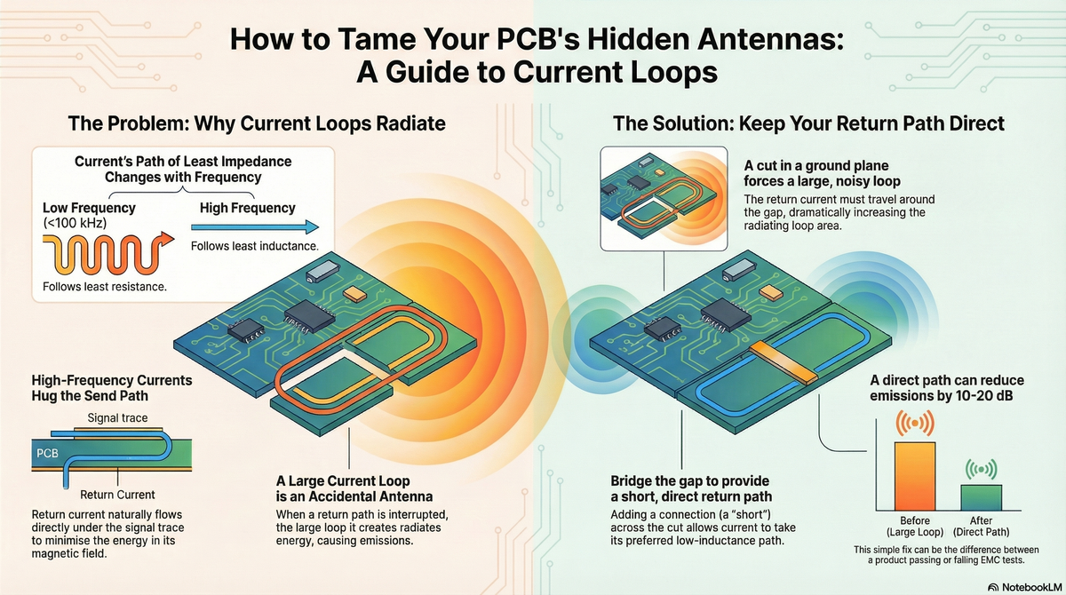
A common misconception, especially for boards with a solid ground plane, is that the return current spreads out evenly across the plane on its way back to the source. It seems logical that the current would take advantage of the massive, low-resistance copper area available. In reality, high-frequency current is much more disciplined.
A simulation detailed in a paper by Dr. Marco Klinger shows this behavior vividly. At a very low frequency of 10 Hz, the return current is spread out. But as the frequency increases to 1 kHz, 10 kHz, and finally 100 kHz, the return current path constricts itself until it flows in a tight, concentrated "shadow" directly underneath the primary signal trace.
This happens because a tight path directly under the signal trace minimizes the total area of the current loop, thereby minimizing the loop's inductance—the path of least impedance at high frequencies. When this natural return path is broken by a gap or cut in the ground plane, the current is forced to make a long detour. This creates a large loop that acts as an efficient antenna, radiating noise. Worse, it creates a shared path for other signals crossing the same gap, leading to increased crosstalk. A demonstration showed that with a large cut in the ground plane, radiated emissions were significant. However, when two buttons—one a direct short, the other capacitively coupled—were pressed to let the current bypass the loop, the emissions harmonics would "drop off significantly."
--------------------------------------------------------------------------------
3. A Tiny "Common-Mode" Leak Can Be More Damaging Than a "Differential-Mode" Flood
Not all currents on your board are created equal. For the purpose of controlling emissions, we can think of them in two categories:
- Differential-Mode: These are the useful currents we want. They flow in a defined loop from a source, through a load, and back again, making our circuits work. They are associated with less-efficient loop antennas.
- Common-Mode: These are unwanted "stray" currents that escape the intended path. They flow together in the same direction on external cables and return via some unintended path, like earth ground. This turns the entire cable into a highly efficient dipole antenna.
The most astonishing takeaway is the disproportionate impact of these two current types. Because the underlying physics makes dipole antennas far more effective radiators at frequencies below 1 GHz, common-mode currents are often the primary cause of EMC failures, even when they are thousands of times smaller than the circuit's functional differential-mode currents.
An excitation frequency of say a hundred megahertz with a common mode current in the order of micro amps that's likely to cause more trouble in terms of emissions than a differential mode current in in the order of milliamps at the same frequency.
This is why controlling tiny, seemingly insignificant stray currents on I/O cables, chassis connections, and power cords is absolutely critical for passing emissions testing. A few microamps of common-mode noise can radiate far more effectively than milliamps of the signal current you're actually trying to manage.
--------------------------------------------------------------------------------
4. In a Power Supply, One Specific Loop Is the Supervillain
Nowhere are these principles more critical than in a switch-mode power supply (SMPS). In any switching circuit, there is one loop that carries current with the highest rate of change (di/dt). This is known as the "critical current loop," and it is the primary source of radiated and conducted noise. Minimizing its size is paramount.
A case study comparing two revisions of a Texas Instruments power supply board provides a stunning example of this principle in action.
- Rev A: The initial 2-layer board layout resulted in a critical current loop with a length of approximately 38 millimeters.
- Rev B: This revision implemented several key improvements. Designers moved to a 4-layer board, added a snubber network to damp ringing, and buried the high-speed gate drive signal on an internal layer for shielding. Crucially, they optimized component placement, more than halving the critical current loop length to just 18 millimeters. This simple change reduced the physical loop area by more than a factor of four.
The measured results of these holistic optimizations were staggering. Compared to the noisy Rev A board, the Rev B board showed a massive reduction in conducted emissions, with improvements of "20 dB" at higher frequencies.
--------------------------------------------------------------------------------
Conclusion: See the Invisible, Control the Unpredictable
Mastering EMC and creating robust electronic designs isn't about memorizing complex equations; it's about learning to visualize the invisible. It’s about seeing the high-frequency current loops that are inherent in every circuit and understanding that at modern switching speeds, you are not just designing a circuit—you are designing a system of miniature antennas. By minimizing the area of these loops, you minimize their ability to radiate and cause problems.
The key is to shift your thinking from simple resistance to high-frequency impedance, from diffuse return paths to concentrated shadows, and from large signal currents to tiny, destructive common-mode currents. Once you start seeing your layout through this lens, you gain control over the unpredictable behavior that plagues so many designs.